Skip to content
DEK PRINTER, Squeegee MPM MOMENTUM ; MPM 125 , MPM MOMENTUM BTB , MPM 100 , MPM EDISON , MPM MOMENTUM HIE ,SPEEDLINE , ITW EAE,MPM SPARE PARTS , MPM UP2000 , MPM ACCUFLEX,MPM ACCELA ,MPM AP EXCEL ,MPM AP , MPM UP3000 , MPM UP1500 , CAMALOT PRODIGY , CAMALOT 8300 , Camalot Dispensers , MPM PRINTER PARTS,GKG PRINTER ,DEK TQ , DEK NeoHorizon 03 iX ,Horizon 03 ix, 265 ,DEK NeoHorizon 01 iX
Introduction
SMT and PCB assembly are critical processes in the manufacturing of electronic devices. As our reliance on electronics grows—driven by advancements in technology and consumer demand—so too does the complexity and sophistication of SMT and PCB assembly. This overview will explore the intricacies of the assembly process, the technological innovations driving improvements, and the market trends shaping the future of electronic manufacturing.
SMT and PCB
Understanding SMT and PCB Assembly
What is SMT?
Surface Mount Technology (SMT) refers to a method for mounting electronic components directly onto the surface of a PCB. Unlike traditional through-hole technology, where components are inserted into holes and soldered on the opposite side, SMT allows for a more compact design, enabling higher component density and reducing the size of electronic devices.
What is PCB?
A Printed Circuit Board is a flat board made of insulating material (usually fiberglass or plastic) on which conductive pathways are etched. These pathways connect different electronic components, allowing them to communicate and function as a cohesive unit. PCBs can be single-sided, double-sided, or multilayered, depending on the complexity of the circuit.
The SMT and PCB Assembly Process
- Design and Prototyping The assembly process begins with the design of the PCB. Engineers use Computer-Aided Design (CAD) software to create layouts that detail the placement of components and the pathways for electrical connections. Prototyping is a critical phase where the initial designs are tested for functionality and manufacturability. Rapid prototyping techniques, such as 3D printing and CNC machining, allow for quick iterations and adjustments based on testing feedback.
- Solder Paste Printing SMT Solder paste printing is the first step in the assembly line. A stencil is used to apply solder paste to specific pads on the PCB. Precision is essential, as the amount and placement of solder paste directly affect the quality of solder joints. Automated stencil printers are commonly employed, ensuring consistent application across multiple boards ,ITW EAE SPEEDLINE mpm printer.
- Component Placement Once the SMT solder paste is applied, the PCB moves to the component placement stage. High-speed pick-and-place machines are used to position components on the board with remarkable accuracy. These machines utilize advanced vision systems to identify component types and locations, ensuring that each part is placed correctly. This stage is critical for maintaining high yield rates, especially for densely populated boards.
- Reflow Soldering After SMT components are placed, the PCB undergoes reflow soldering. The board is passed through a reflow oven, where the solder paste is heated to its melting point, creating solid solder joints between the components and the PCB. The thermal profile of the reflow process is crucial; it must be carefully controlled to avoid issues such as insufficient solder joints or thermal damage to sensitive components.
- Inspection and Testing Following reflow, the assembled PCBs undergo rigorous inspection and testing. Automated Optical Inspection (AOI) systems are commonly used to identify defects, such as misaligned components or insufficient solder. Functional testing may also be conducted to ensure that the PCB operates as intended. This step is vital for maintaining quality and reliability in mass production.
- Encapsulation and Protection Many SMT electronic products require additional protection from environmental factors, leading to encapsulation processes. Techniques such as conformal coating and potting are used to safeguard components from moisture, dust, and mechanical stress. These protective measures are especially important in consumer electronics, automotive applications, and industrial equipment.
- Final Assembly and Packaging Once inspection and testing are complete, the SMT PCBs are integrated into their final product assemblies. This may involve connecting PCBs to other components, such as displays, batteries, or enclosures. Finally, the assembled products are packaged for shipping, often with considerations for minimizing damage during transport.
Technological Innovations
- Miniaturization As electronic devices continue to shrink in size, the demand for compact and efficient SMT PCB designs has increased. Innovations in component packaging, such as System-in-Package (SiP) and Chip-on-Board (CoB) technologies, allow for greater functionality in smaller footprints. This trend is particularly evident in mobile devices, wearables, and IoT products.
- Smart Manufacturing The integration of Internet of Things (IoT) technologies into the manufacturing process has given rise to smart manufacturing. Real-time monitoring and data analytics enable manufacturers to optimize production efficiency, reduce downtime, and minimize waste. Predictive maintenance powered by AI can identify potential equipment failures before they occur, further enhancing reliability.
- Advanced Materials The use of advanced materials in SMT PCB fabrication is also evolving. High-frequency laminates, flexible substrates, and eco-friendly materials are increasingly being utilized to meet specific performance requirements. Additionally, lead-free solder and other environmentally friendly materials are becoming industry standards, driven by regulatory pressures and consumer preferences for sustainable products.
Market Trends
- Demand for Higher Quality With the proliferation of electronic devices, consumers expect higher quality and reliability. SMT Manufacturers are investing in quality assurance measures, including enhanced inspection technologies and process controls, to ensure that every product meets stringent quality standards.
- Rapid Prototyping and Shorter Lead Times The need for faster time-to-market is compelling manufacturers to adopt rapid prototyping techniques and agile production methods. This shift enables companies to respond quickly to market demands and emerging trends, providing a competitive edge.
- Increased Automation Automation is transforming the SMT and PCB assembly landscape. From automated solder paste printing to robotic assembly lines, manufacturers are leveraging automation to improve efficiency and reduce labor costs. This trend is expected to continue, with advancements in robotics and AI enabling more complex and precise assembly operations.
- Global Supply Chain Considerations The global nature of the electronics industry means that manufacturers must navigate complex supply chains. Recent disruptions, such as those caused by the COVID-19 pandemic, have highlighted the importance of supply chain resilience. SMT Companies are increasingly looking to diversify suppliers and invest in local production capabilities to mitigate risks.
Challenges and Solutions
- Complexity of Designs As electronic devices become more complex, so do the designs of PCBs. Managing the intricacies of multilayer boards and high-density interconnects presents challenges in manufacturing and testing. Advanced simulation tools and design-for-manufacturability (DFM) practices can help address these challenges.
- Material Selection The choice of materials can significantly impact performance and reliability. Manufacturers must stay informed about new materials and their properties, balancing cost, performance, and sustainability. Collaborating with suppliers to understand material capabilities can aid in making informed decisions.
- Keeping Pace with Technology The rapid pace of technological change in the electronics industry requires manufacturers to continuously adapt. Ongoing training and skill development for the workforce, along with investment in cutting-edge technologies, are essential for maintaining competitiveness.
Future Outlook
The future of SMT and PCB assembly is promising, driven by ongoing innovations and evolving market demands. As electronics continue to permeate all aspects of life—from consumer devices to industrial applications—manufacturers will need to embrace new technologies, enhance quality control measures, and adopt sustainable practices.
In conclusion, SMT and PCB assembly are at the heart of modern electronics manufacturing. The processes involved are intricate and require precision, advanced technology, and continuous improvement. By understanding and addressing the challenges and opportunities within this field, manufacturers can ensure they remain competitive and responsive to the ever-changing demands of the electronics market.
Various Applications of SMT and PCB Assembly
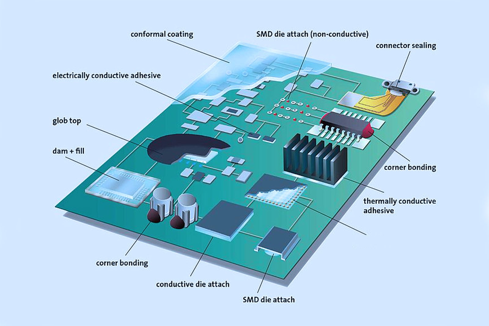
SMT and PCB assembly play a crucial role in the manufacturing of a wide range of electronic devices. These processes not only ensure the proper placement and connection of components but also involve various specialized techniques to enhance the performance, reliability, and longevity of electronic assemblies. This article delves into several key applications within SMT and PCB assembly, including underfill, electronic component pin encapsulation, surface mount adhesive, corner bonding, chip cooling, solder paste, and plasma cleaning.
1. Underfill
Definition and Purpose
Underfill is a polymer material applied to the area underneath an integrated circuit (IC) package, particularly for flip-chip assemblies. The primary purpose of underfill is to enhance the mechanical reliability of the solder joints and provide protection against thermal and mechanical stress. It fills the gap between the IC and the substrate, distributing stress and preventing fatigue over time.
Applications
- Flip-Chip Technology: Underfill is widely used in flip-chip assemblies, where the chip is mounted face down on the PCB. The underfill not only strengthens the connection but also helps in thermal management.
- High-Reliability Applications: Industries such as aerospace, automotive, and medical devices, where failure is not an option, leverage underfill to improve the longevity and robustness of their products.
- Advanced Packaging: In 3D packaging technologies, underfill plays a critical role in maintaining structural integrity as multiple layers of ICs are stacked together.
Types of Underfill
- Capillary Flow Underfills: These rely on capillary action to fill the gaps and are often used for large ICs.
- No-Flow Underfills: These materials are applied before the assembly process and flow during reflow, making them suitable for high-density applications.
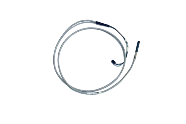
2. Electronic Component Pin Encapsulation
- Definition and Purpose
- Electronic component pin encapsulation involves the application of protective coatings over the pins of electronic components. This process helps to prevent corrosion, contamination, and mechanical damage, enhancing the overall reliability of the components.
- Applications
- Environmental Protection: Encapsulation is vital for components exposed to harsh environments, such as those in automotive and industrial applications, safeguarding against moisture and chemicals.
- Electrical Insulation: Encapsulation materials provide electrical insulation, preventing short circuits and enhancing the safety of electronic devices.
- Mechanical Stability: By providing a protective layer, encapsulation helps maintain the integrity of component pins, reducing the risk of damage during handling and assembly.
- Types of Encapsulation Materials
- Epoxies: Commonly used for their excellent adhesion and mechanical properties.
- Silicones: Offer flexibility and resistance to extreme temperatures, making them suitable for a variety of applications.
SMT
3.Surface Mount Adhesive
Definition and Purpose
Surface mount adhesive is a critical material used to secure components to a PCB during the assembly process. This adhesive helps ensure the stability and reliability of the SMT components, especially in applications where mechanical stress or vibration is a concern.
Applications
- Vibration-Prone Environments: In industries such as aerospace and automotive, where components may be subject to significant vibration, surface mount adhesives provide added mechanical support.
- Thermal Management: Some surface mount adhesives are designed to conduct heat away from components, aiding in thermal management and preventing overheating.
- High-Temperature Applications: Certain adhesives are formulated to withstand high temperatures, making them suitable for applications in automotive and industrial sectors.
Types of Surface Mount Adhesives
- Epoxy-Based Adhesives: Known for their strong bonding properties and durability.
- Acrylic Adhesives: Offer quick curing times and excellent adhesion to various substrates.
4.Corner Bonding
Definition and Purpose
Corner bonding is a technique used to enhance the mechanical stability of electronic components on a PCB. This method involves applying adhesive to the corners of components, effectively creating a “bonding” structure that helps distribute stress and prevent detachment.
Applications
- Enhanced Reliability: Corner bonding is particularly useful in applications where components are subject to thermal cycling or mechanical stresses, such as in automotive and aerospace industries.
- Reduced Stress Concentration: By distributing stress evenly across the component, corner bonding helps minimize the risk of solder joint failure.
- Support for High-Density Assemblies: As SMT PCB designs become more compact, corner bonding provides additional support for components in high-density layouts.
Techniques for Corner Bonding
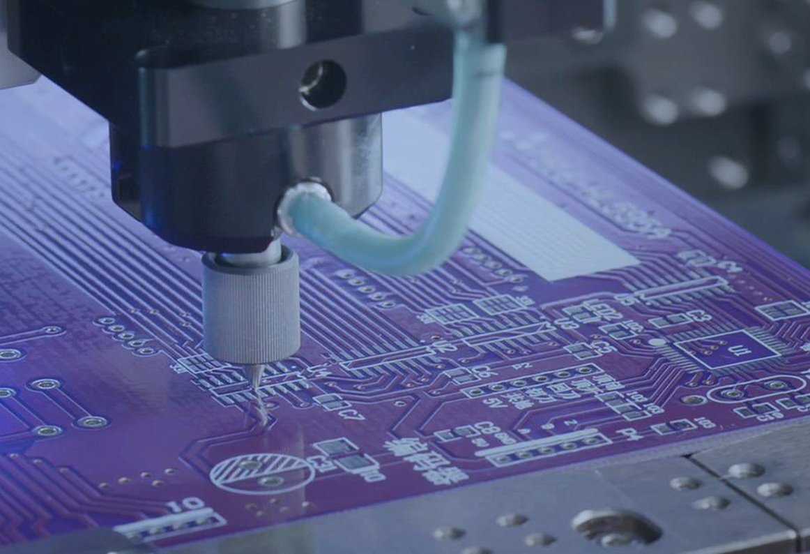
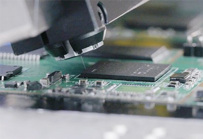
- Automated Dispensing: Precision dispensing systems are used to apply adhesive in controlled amounts, ensuring consistency across assemblies.
- Curing Processes: Adhesives used for corner bonding may require specific curing methods, including heat or UV light, to achieve optimal strength.
5.Chip Cooling
Definition and Purpose
SMT Chip cooling is a critical aspect of electronic design, particularly for high-performance devices that generate significant heat during operation. Effective cooling solutions are essential to maintain optimal performance and prevent thermal damage.
Applications
- High-Power Devices: In applications such as power electronics and high-frequency RF devices, efficient cooling mechanisms are essential to ensure reliability and performance.
- Data Centers: As servers and data centers require effective thermal management to maintain performance, various cooling techniques are employed to manage heat generated by multiple processors.
- Consumer Electronics: Smartphones, laptops, and gaming consoles utilize various cooling methods to ensure optimal performance under heavy load.
Cooling Techniques
- Heat Sinks: Passive cooling solutions that dissipate heat away from components.
- Thermal Interface Materials (TIMs): Materials applied between the chip and heat sink to enhance thermal conductivity.
- Active Cooling Solutions: Fans and liquid cooling systems that actively remove heat from components.
6.Solder Paste
Definition and Purpose
SMT Solder paste is a mixture of solder powder and flux, used to attach surface mount components to PCBs. The paste is applied to the PCB before component placement and is reflowed to create strong electrical connections.
Applications
- Component Assembly: Solder paste is essential for the assembly of SMT components, providing the means to create reliable solder joints.
- Rework and Repair: Solder paste can also be used in repair processes, allowing for rework of defective assemblies.
Types of Solder Paste
- Lead-Based Solder Paste: Traditional paste that provides excellent performance but is increasingly restricted due to environmental regulations.
- Lead-Free Solder Paste: Composed of alternative materials such as tin, silver, and copper, lead-free paste has become the industry standard due to regulatory compliance.
Solder Paste Printing Techniques
- Stencil Printing: The most common method, providing precise control over the amount of paste applied.
- Jet Printing: An emerging technology that allows for selective application of solder paste, reducing waste and enabling high-density applications.
7.Plasma Cleaning
SMT Definition and Purpose
Plasma cleaning is a surface treatment process that utilizes ionized gas (plasma) to remove contaminants from PCB surfaces before assembly. This process enhances adhesion and ensures the reliability of solder joints.
Applications
- Pre-Assembly Cleaning: Plasma cleaning is employed to remove oils, dust, and other contaminants from PCB surfaces, ensuring optimal conditions for soldering.
- Adhesion Improvement: By increasing the surface energy of materials, plasma cleaning enhances the adhesion of adhesives and coatings applied later in the assembly process.
Types of Plasma Cleaning Techniques
- Dielectric Barrier Discharge (DBD): A common plasma cleaning method that generates a low-temperature plasma, suitable for delicate components.
- Reactive Ion Etching (RIE): Used for more aggressive cleaning, this method effectively removes unwanted materials while providing precise control over the etching process.
Conclusion
The applications of SMT and PCB assembly are diverse and vital to the reliability and performance of electronic devices. Techniques such as underfill, electronic component pin encapsulation, surface mount adhesive, corner bonding, chip cooling, solder paste application, and plasma cleaning all contribute to the success of electronic manufacturing. As technology advances, the integration and optimization of these processes will continue to evolve, ensuring that the electronics industry can meet the growing demands for quality, efficiency, and innovation.
This exploration of various applications highlights the intricacies of SMT and PCB assembly, providing insights into how these processes work together to create the reliable electronic products we depend on every day. As SMT manufacturers adopt new technologies and materials, the future of electronic assembly looks promising, with enhanced capabilities and improved performance on the horizon.
With the widespread adoption of electronic products, people’s reliance on electronic devices has been increasing, and the frequency of updates and replacements is relatively high. This not only raises higher fashion requirements for the appearance of products but also demands higher quality.
Currently, whether it’s rigid boards or flexible ones, whether it’s resistors and capacitors or ICs, they all undergo encapsulation, under filling, adhesive reinforcement, and other adhesive operations to ensure product reliability. Especially for mobile phones, the level of dust and waterproofing is increasing, and the precision of adhesive placement is paramount. 3D laser guidance is not only used for graphical guidance but also for tracking the trajectory and shape of the entire dispensing, ensuring that every product produced achieves a 100% yield rate.
Axxon keeps pace with the progress and changes of the times. According to customer requirements, we design products that are more suitable for production, which has been recognized by the market and gained the trust of customers. We strive to provide better services and create more value for our customers.