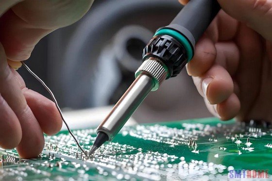
With the miniaturization and precision of electronic products, the application of surface mount technology (SMT) in the electronics manufacturing industry is becoming more and more widespread . In the SMT process , the amount of solder paste directly affects the quality and reliability of the solder joints. In some specific cases, in order to meet specific soldering requirements, we need to increase the amount of solder paste or solder in localized areas.

The need to increase the amount of solder paste or solder locally
In some cases, a localized increase in the amount of solder paste or solder is necessary, and here are some common reasons :
Heat Dissipation : For components that generate a lot of heat, increasing the amount of solder helps to improve heat transfer efficiency.
Mechanical Strength : In areas subject to mechanical stress, increasing the amount of solder can form stronger solder joints.
Compensation for dimensional deviations : Due to deviations in the dimensions of component pins and PCB pads, more solder may be required to ensure a reliable connection.
Localized increase of solder paste or amount of solder
Here are some ways to locally increase the amount of solder paste or solder in the SMT process :
Adjustment of stencil opening size
The amount of solder paste deposited can be directly controlled by adjusting the opening size of the stencil.
Enlarge openings : Increase the size of the stencil openings for pads that require more solder, thus increasing the amount of solder paste deposited.
Use of special shaped openings : Trapezoidal or runway shaped openings can be used to deposit more paste at the edge of the pad.
Advantages : Simple and easy to do, low cost, no need to change the existing process.
Disadvantages : If not done properly, print quality may be compromised; limited by the minimum feature size of the stencil.
Multi-printing
Multiple printings of the same PCB to increase the amount of solder paste deposited.
Advantages : allows precise control of the amount of additional solder; suitable for specific areas where more solder is required.
Disadvantages : Increases production time and cost; may cause printing problems if alignment is not accurate.
Use of solder preforms
Solder preforms are placed on PCB pads prior to reflow soldering.
Advantages : precise control of the amount of solder; suitable for applications requiring large amounts of solder.
Disadvantages : Manual placement is costly and time consuming; automated placement may require additional process steps.
Solder dipping or wave soldering
For through-hole components or specific pads, solder dipping or wave soldering can be used to increase the amount of solder.
Advantages : Adds large amounts of solder quickly and efficiently; suitable for adjustments after reflow soldering.
Disadvantages : Not applicable to all SMT applications; can lead to solder bridging if not properly controlled.
Adjustment of metal content and rheological properties of solder paste
Higher solder volumes can be achieved after reflow by using pastes with higher metal content or different rheological properties.
Advantages : Can be applied to entire boards or selective areas; no stencil design changes required.
Disadvantages : May affect reflow profile and overall process; requires the use of special solder pastes, increasing costs.
The decision to locally increase the amount of solder paste or solder in an SMT process should be carefully considered, balancing the advantages and potential pitfalls. Each method has its own application scenario, and a combination of methods is often required to achieve the goal. Engineers need to evaluate the specific requirements of the assembly process, component characteristics, and the impact on productivity and cost.
What is the typical SMT process ?
The Surface Mount Technology (SMT) process is a widely used method in electronics manufacturing that allows for the efficient assembly of electronic components onto printed circuit boards (PCBs). This process has revolutionized the way electronic devices are made, facilitating miniaturization and increasing production speed. Here’s an overview of the typical SMT process, including its key steps and considerations.
1. PCB Preparation
The process begins with the preparation of the PCB. This includes the design and layout of the circuit, which is typically created using Computer-Aided Design (CAD) software. The PCB is manufactured to the specified design, with pads for surface-mounted components (SMCs) printed on the board. This step ensures that the board has the necessary traces, pads, and vias for electrical connections.
2. Solder Paste Application
Once the SMT PCB is ready, the next step is to apply solder paste to the pads where the components will be placed. Solder paste is a mixture of solder powder and flux. This application is usually done using a MPM printer, which ensures precise and consistent application. The solder paste must be applied evenly to avoid issues during the soldering process.
3. Component Placement
After solder paste application, the next phase is component placement. Automated pick-and-place machines are used to accurately position the SMCs onto the PCB. These machines use vision systems to recognize the components and place them precisely on the solder paste. This step is crucial for ensuring that components are correctly aligned for soldering, which affects the overall quality of the final product.
4. Reflow Soldering
Following component placement, the PCB undergoes reflow soldering, which is typically achieved using a reflow oven. In this step, the assembly is heated to a specific temperature profile. The solder paste melts, allowing the solder to flow and create strong electrical connections between the components and the PCB pads. The temperature profile is critical, as it must be optimized to ensure proper melting and cooling without damaging the components or the PCB.
5. Cleaning
After SMT reflow soldering, some PCBs may require cleaning to remove any flux residues. While many modern solder pastes are formulated to be no-clean, certain applications still benefit from cleaning to enhance reliability and performance. Cleaning can be done using various methods, including aqueous washing or solvent-based cleaning systems.
6. Inspection and Testing
Once the PCBs are assembled and cleaned, they undergo inspection to ensure quality. Automated Optical Inspection (AOI) systems are commonly used to detect defects such as misaligned components, insufficient solder, or other issues. Additionally, functional testing may be performed to ensure that the assembled boards operate as intended.
7. Final Assembly and Packaging
After passing inspection, the PCBs may go through final assembly, which can include the addition of through-hole components, connectors, and enclosures. Finally, the assembled products are packaged for shipment, ready for integration into electronic devices.
Conclusion
The SMT process is characterized by its efficiency, precision, and ability to support high-volume production. As technology continues to advance, so too will the methods and equipment used in SMT, pushing the boundaries of what is possible in electronics manufacturing. Understanding each step of this process is crucial for manufacturers looking to optimize production and maintain high quality in their products.


