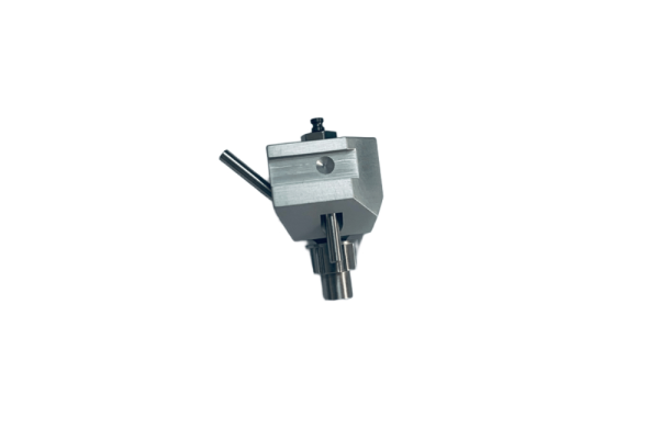
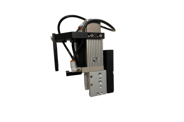
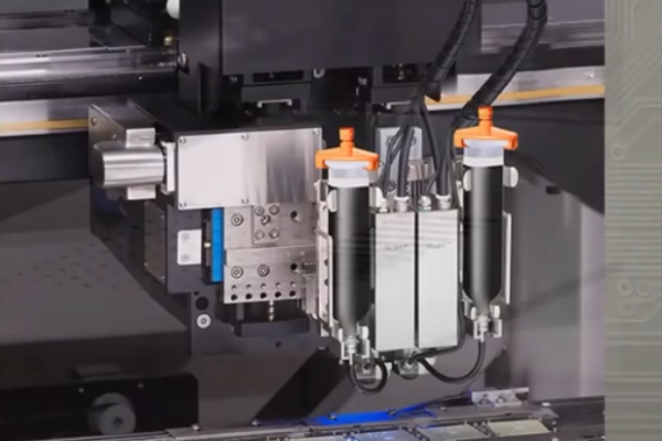
DEK PRINTER, Squeegee MPM MOMENTUM ; MPM 125 , MPM MOMENTUM BTB , MPM 100 , MPM EDISON , MPM MOMENTUM HIE ,SPEEDLINE , ITW EAE,MPM SPARE PARTS , MPM UP2000 , MPM ACCUFLEX,MPM ACCELA ,MPM AP EXCEL ,MPM AP , MPM UP3000 , MPM UP1500 , CAMALOT PRODIGY , CAMALOT 8300 , Camalot Dispensers , MPM PRINTER PARTS,GKG PRINTER ,DEK TQ , DEK NeoHorizon 03 iX ,Horizon 03 ix, 265 ,DEK NeoHorizon 01 iX

1. Introduction to Semiconductors
Semiconductors are materials whose electrical conductivity is intermediate between that of conductors and insulators at room temperature. This unique property arises from the structure of semiconductor materials, which typically include silicon (Si), germanium (Ge), and gallium arsenide (GaAs). Semiconductors are essential in modern electronics and form the backbone of numerous technologies.
Their ability to be manipulated through doping—introducing impurities to change electrical properties—enables the creation of p-type and n-type semiconductors, essential for forming p-n junctions. This property allows for the fabrication of various devices, including diodes and transistors, critical for electronic circuits.
2. Applications of Semiconductors
Semiconductors are integral to many sectors:
- Consumer Electronics: Smartphones, tablets, and laptops rely heavily on semiconductors for processing, display, and connectivity. Integrated circuits (ICs) and microprocessors are core components in these devices.
- Automotive Industry: Modern vehicles are equipped with numerous semiconductor devices that manage everything from engine control units to advanced driver-assistance systems (ADAS). The rise of electric vehicles further accelerates semiconductor demand.
- Military and Aerospace: High-reliability semiconductors are crucial in defense systems, avionics, and communication technologies. They must withstand harsh environments while maintaining performance.
- Industrial Applications: In manufacturing and automation, semiconductors are used in sensors, control systems, and robotics, enhancing efficiency and precision.
- LED Technology: Light-emitting diodes (LEDs) utilize semiconductor materials to produce light efficiently, leading to widespread adoption in lighting and displays.
- MEMS (Micro-Electro-Mechanical Systems): These devices combine mechanical and electrical components on a microscopic scale, finding applications in sensors, actuators, and more.
- Electroacoustics: Semiconductors are vital in microphones and speakers, enabling high-quality sound reproduction.
3. Types of Semiconductor Devices
- Diodes: Semiconductor diodes allow current to flow in one direction, making them essential in rectifying AC to DC. Varieties include zener diodes for voltage regulation and Schottky diodes for fast switching.
- Transistors: The building blocks of modern electronics, transistors act as switches or amplifiers. Bipolar junction transistors (BJTs) and field-effect transistors (FETs) are the most common types, each serving distinct functions in circuits.
- Integrated Circuits (ICs): ICs combine multiple semiconductor devices into a single package, enabling complex functions in a compact form. Analog and digital ICs cater to different applications, from signal processing to computation.
4. Semiconductor Manufacturing Processes
The semiconductor manufacturing process is intricate and involves several critical steps:
- Front-End Processes:
- Circuit Design: Engineers use electronic design automation (EDA) tools to create complex circuit layouts, optimizing performance and efficiency.
- Coating: Photoresist materials are applied to wafers, forming a thin layer that can be selectively removed in later steps.
- Etching: Techniques like dry and wet etching define the circuit patterns on the wafer, shaping the microscopic features of the devices.
- Slicing: Wafers are sliced from a single crystal ingot, followed by polishing to create a smooth surface for further processing.
- Back-End Processes:
- Surface Mount Technology (SMT): This assembly process involves placing components onto the surface of PCBs. SMT enhances manufacturing efficiency and reduces footprint.
- Packaging: Various packaging types, such as dual in-line packages (DIPs) and ball grid arrays (BGAs), protect the semiconductor and facilitate connection to other components.
- Testing: Rigorous testing ensures reliability and performance, with methods ranging from electrical testing to environmental stress tests.
5. Dispensing Process in Semiconductor Packaging
The dispensing process is critical in semiconductor packaging, involving the precise application of adhesives:
- Chip Fixation – Red Glue: This epoxy adhesive provides strong bonding between the die and substrate, ensuring structural integrity.
- Electrical Connection Fixation – Silver Paste: Silver paste is used to create electrical connections, particularly in flip-chip bonding, where efficiency and heat dissipation are vital.
- Fixing MEMS Devices – Silicone: Silicone adhesives provide flexibility and protection for MEMS devices, accommodating potential movement or vibrations.
- COB Packaging Protection – Epoxy Glue: Used in chip-on-board (COB) applications, epoxy glue encapsulates chips, protecting them from environmental damage.
- Chip Solder Ball Protection (Underfill): Underfill epoxy is applied to enhance mechanical strength and thermal performance, critical in high-stress applications.
6. Challenges and Innovations in Semiconductor Technology
The semiconductor industry faces several challenges:
- Material Costs: The rising costs of raw materials can affect profitability and pricing strategies.
- Supply Chain Disruptions: Global events, such as pandemics or geopolitical tensions, can disrupt supply chains, leading to shortages.
- Environmental Impact: The production process has significant environmental implications, prompting a shift toward sustainable practices.
- Technological Innovations: Advancements in materials, such as new semiconductor compounds and processes, are essential for meeting the demands of emerging technologies like AI and IoT.
7. Future Trends in the Semiconductor Industry
Looking ahead, several trends are shaping the semiconductor landscape:
- Miniaturization: The push for smaller, more powerful devices continues, driving innovations in chip design and fabrication.
- IoT Integration: The rise of the Internet of Things (IoT) necessitates semiconductors that support connectivity and efficiency.
- Flexible Electronics: Advances in materials are enabling the development of flexible and wearable devices, expanding the application of semiconductors.
- Quantum Computing: This emerging field relies on novel semiconductor technologies to enable new computational paradigms.
- 5G Technology: The rollout of 5G networks is increasing demand for advanced semiconductors capable of supporting high-speed communication.
8. Conclusion
Semiconductors are fundamental to modern technology, enabling advancements across various industries. Their unique properties and versatility make them indispensable in the development of electronic devices, from consumer products to sophisticated aerospace systems. As the industry navigates challenges and embraces innovations, the future of semiconductors promises exciting developments that will continue to shape the world.
Various applications of semiconductors
Flip Chip Underfill
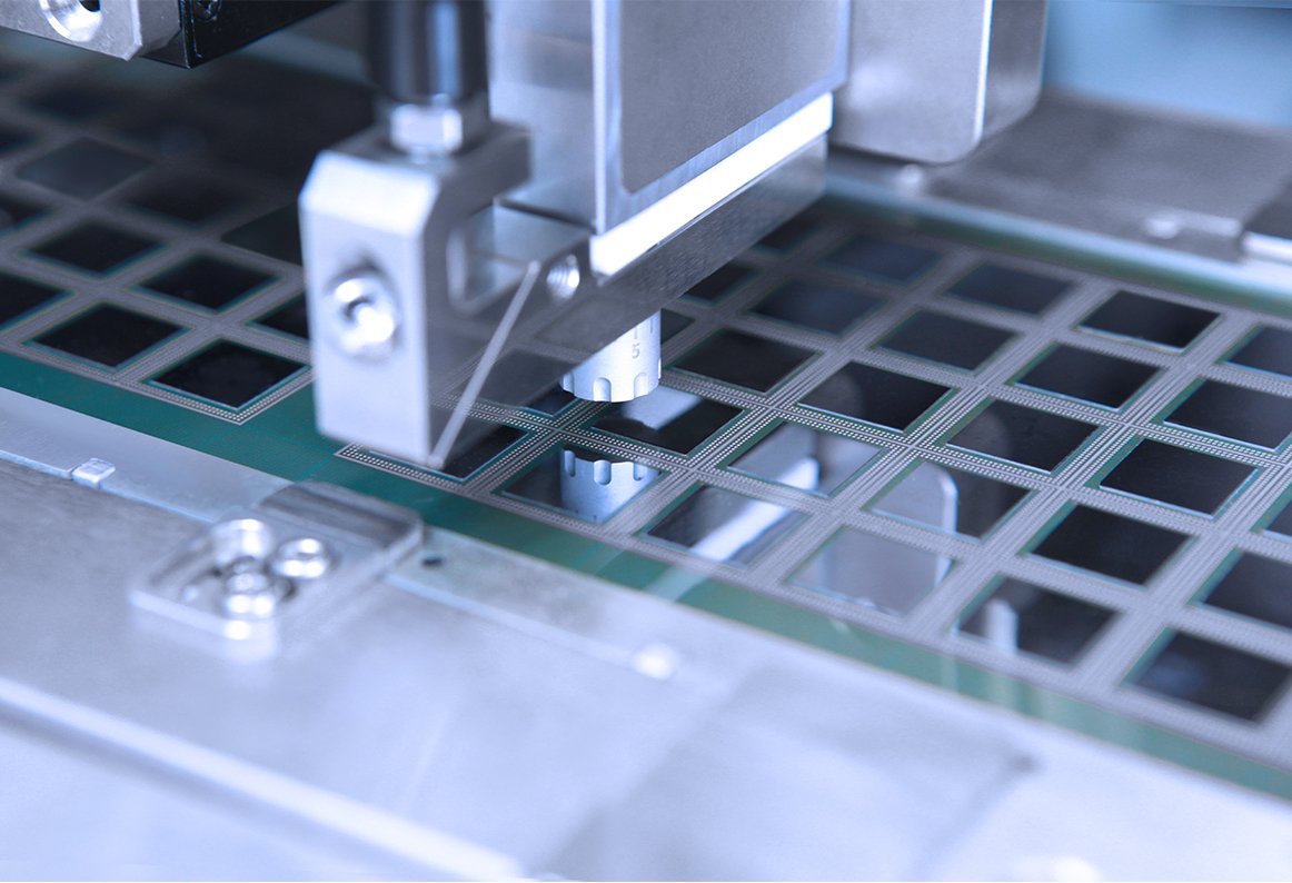
Flip chip technology has become a crucial component in the semiconductor packaging landscape, particularly for high-density applications. This method allows for direct bonding of the chip to the substrate, enabling better electrical performance and heat dissipation. However, the underfilling process is vital for enhancing reliability and performance, especially in preventing mechanical failures and ensuring robust connections.
1. Control of Overflow Width
One of the critical aspects of the underfilling process is managing the overflow width. Given the dense arrangement of components around the perimeter of flip chip packages, any excess adhesive can lead to several issues:
- Short Circuits: Overflowing adhesive can bridge connections between adjacent solder bumps, potentially leading to electrical shorts.
- Aesthetic Quality: Excess material can affect the visual appeal of the final product, which is especially important for consumer electronics.
- Thermal Management: An uncontrolled overflow can disrupt thermal dissipation paths, affecting device performance under load.
To address these concerns, precise control mechanisms are implemented during the dispensing process:
- Dispensing Technology: Employing high-precision dispensing systems (such as jetting or time-pressure dispensing) helps manage the volume and placement of the underfill material.
- Process Parameters: Variables like dispensing speed, nozzle size, and adhesive viscosity are finely tuned to minimize overflow while ensuring adequate filling.
- Inspection Techniques: Post-dispensing inspections, such as optical or X-ray imaging, can detect overflow and inform adjustments to the process in real-time.
2. Surface Preparation and Dispense Accuracy
The smooth surface of BGA (Ball Grid Array) chips presents unique challenges during the underfill process. The need for high accuracy in dispense points is paramount, as any misalignment can result in inadequate coverage or contamination.
- Surface Cleaning: Prior to underfilling, the chip surface must be meticulously cleaned to remove any contaminants, including dust, oils, and residues. Common cleaning methods include solvent cleaning or plasma treatment to enhance adhesion.
- Precision Dispensing: Achieving accurate dispense points is essential for ensuring the adhesive flows correctly around the solder balls. Technologies like automated vision systems can guide the dispensing head to precise locations, compensating for any alignment variations.
- Consistency in Material Flow: The adhesive’s rheological properties—such as viscosity and flow characteristics—are critical. High-viscosity adhesives may not flow well into tight spaces, leading to incomplete underfilling. Properly formulated materials help ensure smooth and even distribution.
Maintaining a clean, controlled environment during the dispensing process is vital to prevent defects and ensure consistent results.
3. Addressing Solder Ball Arrangement and Voids
BGA chips typically have solder balls arranged in a non-uniform pattern, leading to potential void formation during the underfilling process. Voids can significantly impact the reliability of the connection and the overall performance of the device.
- Understanding Void Formation: Voids can occur due to several factors:
- Air Entrapment: As the adhesive flows into the underfill cavity, air can become trapped, leading to voids if not adequately managed.
- Viscosity Changes: Variations in adhesive viscosity, influenced by temperature and process conditions, can affect how the material flows and fills the space around the solder balls.
- Mitigation Strategies:
- Controlled Heating: Applying controlled heat during the underfill process can help lower the adhesive’s viscosity, promoting better flow and reducing the risk of voids. However, this must be carefully managed to avoid overheating, which can degrade the adhesive.
- Vacuum Filling Techniques: Utilizing vacuum systems during the dispensing can help evacuate air pockets, ensuring more complete filling around the solder balls.
- Material Selection: Choosing underfill materials with optimal flow properties is crucial. Low-viscosity adhesives can enhance flow into tight spaces, minimizing voids.
Regular monitoring of the underfill process is necessary to detect and correct void-related issues, ensuring long-term reliability.
4. Impact of Machine Heating on Adhesive Viscosity
The viscosity of the adhesive used in the underfill process is influenced by temperature, and this factor must be meticulously controlled to ensure optimal dispensing performance.
- Viscosity and Dispensing Volume: The viscosity of the adhesive directly affects the volume dispensed. Higher temperatures typically lower viscosity, allowing the adhesive to flow more easily. Conversely, cooler temperatures can lead to thicker, more difficult-to-dispense materials.
- Heating Mechanisms: Many underfill machines incorporate heating elements at the bottom to maintain adhesive viscosity within a specific range. However, this heating must be carefully calibrated:
- Uniform Heating: Uneven heating can result in variations in viscosity, leading to inconsistent dispensing volumes and patterns. Ensuring even heat distribution is critical.
- Temperature Monitoring: Advanced systems often include temperature sensors that provide real-time feedback, allowing operators to adjust settings dynamically based on viscosity changes.
- Adhesive Properties: Selecting adhesives with stable viscosity across a range of temperatures can enhance process reliability. Manufacturers often provide viscosity data at different temperatures to help select the best material for specific applications.
5. Conclusion
The Semiconductor flip chip underfilling process is a complex yet critical aspect of semiconductor packaging that ensures the reliability and performance of modern electronic devices. By controlling overflow width, ensuring precise dispense accuracy, mitigating void formation, and managing adhesive viscosity through controlled heating, manufacturers can significantly enhance the effectiveness of the underfill process.
As technology continues to evolve, the need for advanced materials and dispensing techniques will grow. Innovations in adhesive formulations and dispensing technologies will likely play a pivotal role in addressing the challenges posed by increasing device complexity and miniaturization.
Future research will focus on optimizing underfill processes to further reduce defects and enhance performance, ensuring that flip chip technology remains a cornerstone of high-density electronic applications.
Dome Coating
Introduction
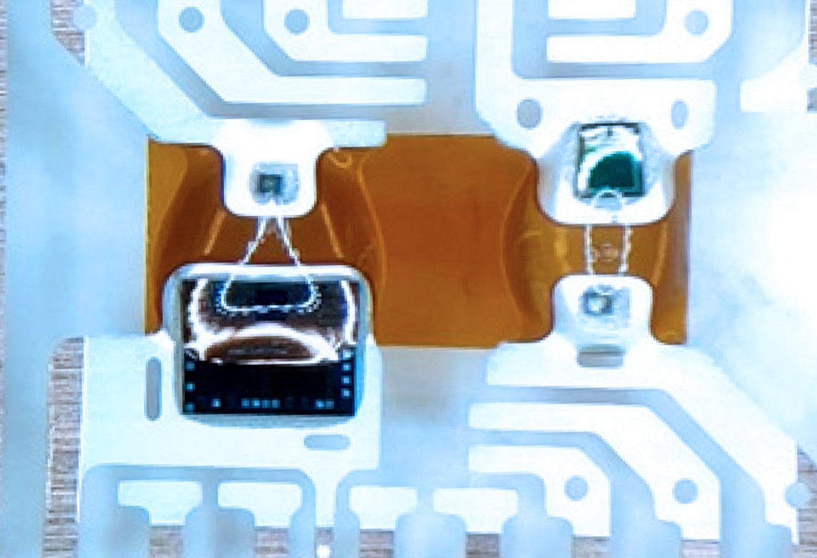
Dome coating is a protective method primarily used in semiconductor packaging to safeguard multiple chips and wires on leadframes. This technique enhances the durability and reliability of electronic components by providing a robust barrier against environmental factors.
Application and Process
Dome coating is commonly applied to the front side of leadframes, with the adhesive flowing through the gaps to coat both sides. Here’s a detailed look at the process:
- Surface Preparation: Before applying the dome coating, the leadframe surfaces must be thoroughly cleaned to remove any contaminants, such as dust, oils, or residues. This step is crucial for ensuring strong adhesion between the adhesive and the substrate.
- Dispensing Adhesive:
- Dispensing Techniques: Various dispensing methods can be employed, including time-pressure dispensing, jet dispensing, or syringe dispensing. The choice of technique depends on factors such as the required precision and the viscosity of the adhesive.
- Controlled Flow: The adhesive is dispensed onto the front side of the leadframe, filling the gaps between the chips and wires. The design of the leadframe and the adhesive’s flow characteristics ensure that the coating penetrates adequately, reaching the backside.
- Curing Process: After dispensing, the adhesive must cure to form a solid protective layer. Curing can occur through heat, UV light, or ambient conditions, depending on the adhesive formulation. Proper curing ensures the adhesive achieves its full mechanical and chemical properties.
- Thickness Control: Achieving the right adhesive thickness is critical for effective protection. The coating should be thick enough to shield against moisture, dust, and mechanical stress but not so thick as to add unnecessary weight or interfere with other components.
Benefits of Dome Coating
Dome coating offers several advantages for semiconductor packaging:
- Enhanced Protection: The primary benefit of dome coating is the protection it provides to chips and wires. The adhesive forms a barrier against environmental factors such as moisture, dust, and chemicals, which can degrade performance and reliability over time.
- Increased Lifespan: By protecting components from physical damage and corrosion, dome coating can significantly extend the lifespan of electronic devices. This is particularly important in applications where longevity is crucial, such as automotive and aerospace electronics.
- Mechanical Support: The adhesive layer provides additional mechanical support, helping to absorb stress during thermal cycling and reducing the risk of cracks or failures in solder joints.
- Electrical Insulation: Many adhesives used in dome coating have excellent electrical insulating properties, helping to prevent short circuits and other electrical failures.
- Aesthetic Appeal: Dome coating can enhance the visual appearance of electronic assemblies, providing a uniform finish that can be important for consumer products.
Challenges and Considerations
While dome coating is beneficial, several challenges must be addressed:
- Adhesive Selection: Choosing the right adhesive is critical for achieving the desired performance. Factors to consider include adhesion strength, curing time, viscosity, and thermal stability. Incompatible adhesives can lead to adhesion failures or degraded performance.
- Process Control: Maintaining consistent dispensing parameters is essential to ensure uniform coating thickness. Variations in dispensing speed, pressure, or adhesive viscosity can lead to uneven coatings, which may compromise protection.
- Curing Conditions: Proper curing is vital for achieving optimal adhesive properties. Inadequate curing can lead to weak bonds and compromised protection. Monitoring environmental conditions (temperature, humidity) during the curing process is crucial.
- Environmental Impact: The choice of adhesive can also have environmental implications. Using low-VOC (volatile organic compound) adhesives can reduce the environmental footprint of the coating process.
- Inspection and Quality Control: Post-coating inspection is essential to ensure the integrity of the dome coating. Techniques such as visual inspection, thickness measurement, and adhesive bond testing can help identify defects.
Conclusion
Semiconductor Dome coating is a vital technique in semiconductor packaging, providing essential protection for chips and wires on leadframes. By ensuring proper adhesive selection, precise dispensing, and controlled curing conditions, manufacturers can leverage dome coating to enhance the durability and reliability of electronic components.
As technology advances, the demand for more effective and environmentally friendly coating solutions will continue to grow. Innovations in adhesive formulations and application techniques will play a crucial role in the future of dome coating, ensuring that electronic devices meet the evolving needs of consumers and industries alike.
Dam & Fill
Introduction
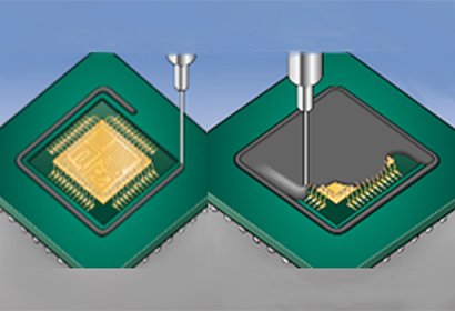
The Semiconductor Dam & Fill process is a crucial technique in semiconductor packaging that enhances the protection of sensitive components. By utilizing a dual-valve dispensing system, this method ensures optimal encapsulation of dies or chips, safeguarding them against environmental factors and mechanical stress.
1. Process Overview
The Dam & Fill process involves two distinct phases facilitated by a dual-valve dispensing system:
- Dam Formation:
- High-Viscosity Adhesive: The first valve dispenses a high-viscosity adhesive around the perimeter of the die or chip, forming a dam. This adhesive acts as a barrier that contains the filling material and prevents it from overflowing.
- Control of Adhesive Flow: Accurate control of the dispensing parameters, including speed and pressure, is essential to ensure that the dam is formed uniformly and effectively. The high viscosity of the adhesive allows for precise placement without the risk of it flowing away.
- Filling:
- Low-Viscosity Adhesive: Once the dam is established, the second valve introduces a low-viscosity adhesive into the cavity created by the dam. This adhesive flows easily, filling the space around the die and ensuring complete coverage.
- Effective Encapsulation: The low-viscosity adhesive flows into tight spaces, encapsulating the die thoroughly. This ensures that all exposed areas are protected, reducing the risk of moisture ingress or mechanical damage.
2. Applications of Dam & Fill
The Dam & Fill technique is widely used in various semiconductor packaging applications, including:
- Semiconductor Packaging: This process is crucial in encapsulating chips, protecting them from environmental contaminants and physical stress. It enhances the reliability and longevity of semiconductor devices.
- Wire Bonding Encapsulation: In wire bonding applications, Dam & Fill protects the delicate wire bonds from damage and corrosion, ensuring reliable electrical connections.
- Smart Card Chip Packaging: Smart cards, used for secure transactions and access control, benefit from the Dam & Fill process to encapsulate their chips, safeguarding them from physical wear and environmental exposure.
- Touch Panel (TP) Screen Bonding: The Dam & Fill process is employed in bonding layers of touch panels, providing an effective seal that protects the sensitive electronic components beneath the screen.
3. Benefits of Dam & Fill
The Dam & Fill process offers several advantages that make it a preferred choice in many applications:
- Effective Protection: By encapsulating the die or chip, the Dam & Fill process provides a robust barrier against moisture, dust, and other contaminants. This is crucial for maintaining the operational integrity of semiconductor devices.
- Increased Longevity: The protective layer formed through the Dam & Fill process prolongs the lifespan of components by preventing physical damage and degradation from environmental factors.
- Enhanced Mechanical Stability: The dual adhesive approach ensures that the die is securely anchored, reducing the risk of movement during thermal cycling or mechanical stress. This stability is essential for maintaining performance over time.
- Versatility: The Dam & Fill process can be adapted for various applications, including different chip sizes, shapes, and types of adhesives, making it a flexible solution for many packaging needs.
- Improved Yield Rates: By minimizing defects and ensuring thorough encapsulation, the Dam & Fill process can enhance production yield, reducing waste and improving cost-effectiveness.
4. Challenges and Considerations
Despite its advantages, the Dam & Fill process also presents several challenges that manufacturers must address:
- Adhesive Selection: Choosing the appropriate adhesives for both the dam and fill phases is critical. The high-viscosity adhesive must form a secure barrier, while the low-viscosity adhesive should flow well and provide effective coverage. Compatibility between adhesives is essential to avoid performance issues.
- Process Control: Maintaining consistent dispensing parameters is crucial to achieving uniform results. Variations in pressure, speed, or temperature can lead to defects, such as incomplete encapsulation or adhesive overflow.
- Curing Conditions: The curing process for both adhesives must be carefully controlled to ensure optimal performance. Factors such as temperature and humidity can affect curing times and adhesive properties.
- Inspection and Quality Control: Post-application inspections are essential to verify the integrity of the encapsulation. Techniques such as X-ray inspection and optical scanning can help identify defects or voids in the adhesive layer.
- Environmental Impact: The choice of adhesives and the curing process can have environmental implications. Manufacturers are increasingly seeking low-VOC (volatile organic compound) adhesives to reduce their environmental footprint.
Conclusion
The Semiconductor Dam & Fill process is a vital technique in semiconductor packaging, providing effective encapsulation that enhances the durability and reliability of electronic components. By employing a dual-valve system to dispense high- and low-viscosity adhesives, manufacturers can achieve optimal protection against environmental factors and mechanical stress.
As technology continues to evolve, the demand for effective and reliable packaging solutions will grow. Innovations in adhesive formulations and dispensing technologies will play a crucial role in the future of the Dam & Fill process, ensuring that semiconductor devices meet the increasing performance and reliability standards of modern applications.
No-flow Underfill
Introduction
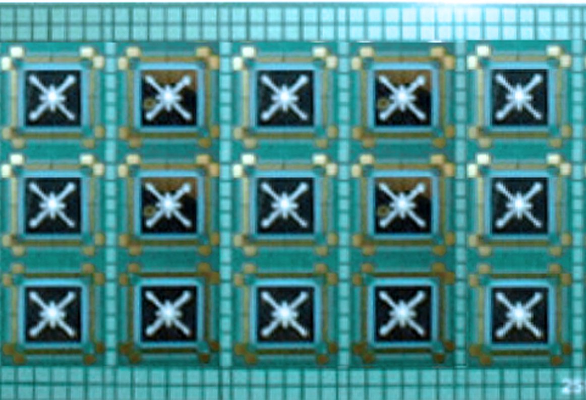
Semiconductor No-flow underfill (NFU) is a critical adhesive technology used primarily in the packaging process of flip-chip devices. This method is essential for enhancing the mechanical stability and thermal performance of semiconductor components. NFU is designed to flow and cure without the need for additional heating during the assembly process, making it a versatile choice for various applications.
1. Process Overview
The no-flow underfill process involves several key steps:
- Material Composition:
- NFU materials are typically formulated from epoxy resins that are engineered to maintain a high viscosity before curing. This viscosity prevents the adhesive from flowing during the assembly process, hence the name “no-flow.”
- The materials often include fillers to enhance thermal conductivity and mechanical strength while ensuring that the underfill remains stable and does not flow into undesired areas.
- Dispensing Process:
- Volume Control: Precise control over the volume of adhesive dispensed is critical. Too little adhesive may lead to incomplete coverage, while too much can create excess that may flow into areas where it is not needed.
- Dispensing Path: The path taken by the dispensing nozzle must be carefully planned to ensure consistent application across the chip. This helps avoid air bubbles and ensures even thickness throughout the underfill layer.
- Valve Parameters: The dispensing system typically employs advanced valve technologies that allow for fine adjustments in pressure, timing, and speed. This precision is essential for maintaining the integrity of the coverage.
- Curing Process:
- After dispensing, the NFU material cures at room temperature or through a controlled heating process, depending on the specific formulation. The curing process solidifies the adhesive, creating a robust bond between the chip and substrate.
2. Applications of No-Flow Underfill
No-flow underfill is used in various applications, including:
- Flip-Chip Packaging: NFU is predominantly employed in flip-chip assemblies, where chips are mounted face down onto substrates. The adhesive provides excellent mechanical support and thermal conductivity, ensuring reliable connections.
- High-Performance Electronics: Devices requiring high reliability and performance, such as smartphones, computers, and automotive electronics, benefit from NFU due to its robust encapsulation properties.
- MEMS Devices: In Micro-Electro-Mechanical Systems (MEMS), NFU provides effective protection against environmental factors, enhancing the longevity and performance of these sensitive components.
- LED Packaging: No-flow underfill is also used in LED packaging to improve heat dissipation and protect the chip from moisture, thereby enhancing the overall lifespan of the device.
3. Benefits of No-Flow Underfill
The use of no-flow underfill offers several advantages:
- Enhanced Mechanical Stability: NFU provides a solid bond between the die and the substrate, improving resistance to thermal cycling and mechanical stress. This is crucial in maintaining performance over time.
- Reduced Voids and Air Bubbles: The controlled dispensing process minimizes the risk of air entrapment, which can lead to voids that compromise the integrity of the underfill layer.
- Improved Thermal Performance: NFU materials often have high thermal conductivity, facilitating effective heat dissipation from the chip. This helps in maintaining optimal operating temperatures, enhancing device performance.
- Simplified Processing: The no-flow characteristic of these underfills allows for easier handling during assembly, reducing the risk of misalignment and making the process more efficient.
- Compatibility with Advanced Packaging: NFU is well-suited for modern, high-density packaging techniques, making it a preferred choice for manufacturers focusing on miniaturization and performance.
4. Challenges and Considerations
While no-flow underfill presents numerous advantages, several challenges need to be addressed:
- Material Selection: The choice of the right NFU formulation is critical. Factors such as viscosity, curing time, and thermal properties must align with specific application requirements to ensure optimal performance.
- Process Control: Maintaining consistent dispensing parameters is essential. Variations in temperature, pressure, or dispensing speed can lead to inconsistent application, affecting coverage and performance.
- Curing Conditions: The curing process must be carefully monitored. Inadequate curing can result in weak bonds and compromised protection. It is essential to follow manufacturer recommendations for curing times and temperatures.
- Inspection and Quality Control: Post-application inspections are vital to verify the integrity of the underfill. Techniques such as X-ray imaging and optical inspection can help detect defects or inconsistencies.
- Environmental Considerations: The use of low-VOC and environmentally friendly NFU materials is becoming increasingly important as regulations tighten. Manufacturers must consider the environmental impact of their adhesive choices.
Conclusion
Semiconductor No-flow underfill is an essential technology in semiconductor packaging, particularly for flip-chip devices. By employing a dual-valve dispensing system that controls adhesive volume, path, and valve parameters, manufacturers can achieve effective encapsulation, ensuring the reliability and longevity of electronic components.
As the demand for high-performance electronics continues to rise, innovations in no-flow underfill formulations and dispensing technologies will play a pivotal role in enhancing packaging solutions. The ongoing development of materials that offer superior thermal management and mechanical stability will ensure that no-flow underfill remains a vital component in the future of semiconductor packaging.
Glob Top
Introduction
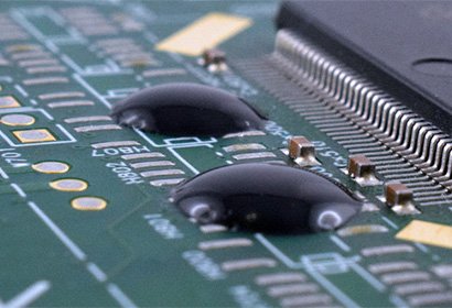
Semiconductor Glob top encapsulation is a widely used method for protecting semiconductor components on printed circuit boards (PCBs), particularly after surface mounting and wire bonding. This technique offers significant flexibility in design and is essential for enhancing the durability and reliability of electronic devices.
1. Process Overview
The glob top process involves several key steps:
- Material Selection:
- Sealants: Glob top encapsulants are typically made from epoxy or silicone-based materials, chosen for their excellent adhesion, thermal stability, and protective properties. These materials are designed to provide a robust barrier against environmental factors such as moisture, dust, and mechanical stress.
- Surface Preparation:
- Before application, the PCB surface must be cleaned to remove contaminants that could interfere with adhesion. This may involve solvent cleaning or plasma treatment.
- Dispensing Process:
- Dispensing Methods: The glob top material can be applied using various methods, including syringe dispensing, jetting, or screen printing. The choice of method depends on factors like the desired precision and the viscosity of the encapsulant.
- Application: The glob top material is applied directly over the die and bond wires, forming a protective dome. This application must be precise to ensure complete coverage without excessive overflow.
- Curing Process:
- After dispensing, the glob top material must cure, typically through heat or UV light. Proper curing is essential for achieving the desired mechanical and thermal properties.
2. Applications of Glob Top
Glob top encapsulation is commonly used in various applications, including:
- Chip-On-Board (COB) Packaging: In COB assemblies, glob top provides a protective layer over the chip and bond wires, enhancing durability and reliability.
- Consumer Electronics: Devices such as smartphones, tablets, and wearables utilize glob top encapsulation to protect sensitive components from environmental damage.
- Automotive Electronics: The robust protection offered by glob top materials is critical for automotive applications, where components are exposed to harsh conditions.
- Medical Devices: In medical technology, glob top encapsulation ensures the reliability of electronic components used in critical applications, providing a barrier against moisture and contamination.
3. Benefits of Glob Top
The glob top encapsulation process offers numerous advantages:
- Enhanced Protection: Glob top materials provide excellent protection against moisture, dust, and physical damage, significantly extending the lifespan of electronic components.
- Design Flexibility: The ability to encapsulate components after surface mounting allows for greater design flexibility, making it easier to adapt to changes during the manufacturing process.
- Improved Thermal Performance: Many glob top materials have good thermal conductivity, helping to dissipate heat generated by the components, which is crucial for maintaining optimal operating conditions.
- Electrical Insulation: Glob top encapsulants offer excellent electrical insulation, reducing the risk of short circuits and enhancing the reliability of the assembly.
- Reduced Risk of Mechanical Stress: The protective layer provided by glob top materials helps absorb mechanical stress, minimizing the risk of damage during thermal cycling or handling.
4. Challenges and Considerations
Despite its benefits, glob top encapsulation presents several challenges:
- Material Compatibility: Selecting the right encapsulant is crucial. Factors such as adhesion to substrates, thermal properties, and curing conditions must align with specific application requirements.
- Dispensing Precision: Achieving accurate and uniform application is critical. Variations in dispensing parameters can lead to defects, such as incomplete coverage or excessive overflow.
- Curing Conditions: The curing process must be carefully controlled. Inadequate curing can result in weak bonds or compromised protection, while excessive heat can damage sensitive components.
- Inspection and Quality Control: Post-application inspections are essential to verify the integrity of the glob top layer. Techniques such as X-ray imaging and optical inspection can help identify defects.
- Environmental Impact: The choice of materials can have environmental implications. Manufacturers are increasingly looking for low-VOC and eco-friendly encapsulants to minimize their environmental footprint.
Conclusion
Semiconductor Glob top encapsulation is an essential process in the protection of semiconductor components on printed circuit boards. By providing a robust barrier against environmental factors, glob top materials enhance the durability and reliability of electronic devices, making them suitable for a wide range of applications.
As technology advances, the demand for effective and environmentally friendly encapsulation solutions will continue to grow. Innovations in glob top materials and dispensing techniques will play a vital role in improving packaging solutions, ensuring that electronic devices meet the evolving needs of industries and consumers alike.
Silver Paste
1. Uniform Coating of Silver Paste
Achieving a uniform coating of silver paste is crucial for effective electrical connections. This involves:
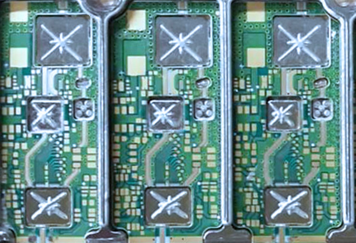
- Surface Preparation: Ensuring that the substrate and IC surfaces are clean and free of contaminants to promote good adhesion.
- Dispensing Techniques: Utilizing precise dispensing methods such as screen printing, syringe dispensing, or jetting to ensure consistent application across the bonding area.
- Viscosity Control: Maintaining the correct viscosity of the silver paste to facilitate even flow during application, which helps prevent issues like uneven thickness or gaps in the coating.
2. Stability of Dispensing from the Valve
Stability in dispensing is essential for reliable connections, which includes:
- Valve Calibration: Regularly calibrating dispensing valves to ensure consistent pressure and flow rates, minimizing variations that could affect paste application.
- Monitoring Parameters: Keeping an eye on factors such as temperature and humidity, as these can influence the performance of the silver paste and the dispensing process.
- Quality Control: Implementing rigorous inspection processes to verify the consistency and stability of the silver paste application, ensuring that each connection meets required specifications.
Conclusion
By focusing on uniform coating and stable dispensing, the use of Semiconductor silver paste in connecting ICs to substrates can enhance electrical performance and reliability, critical for high-performance electronics.
Chip-level Solder Paste
Introduction
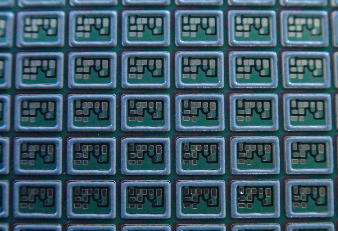
Semiconductor Chip-level solder paste application is a critical step in the assembly of electronic components on printed circuit boards (PCBs). This process involves applying solder paste to connect integrated circuits (ICs) to substrates, ensuring reliable electrical connections and mechanical stability. Key factors that influence the effectiveness of solder paste application include the uniformity of dispensing dots and precise control of dispensing height. This overview will delve into these aspects and their implications for the soldering process.
1. Uniformity of Solder Paste Dispensing Dots
Uniformity in solder paste dispensing is crucial for several reasons:
- Consistency in Solder Joints:
- Uniform dispensing ensures that each solder joint has the appropriate amount of paste, which is vital for achieving reliable electrical connections. Variations in paste volume can lead to cold solder joints, insufficient connections, or bridging between pads.
- Auger Valve Technology:
- The auger valve is a preferred choice for solder paste dispensing due to its ability to provide stable control over the dispensing volume. The auger mechanism allows for precise movement of solder paste, ensuring that each dot is consistently sized.
- Advantages of Auger Valves:
- Consistency: The auger valve minimizes variability in the amount of paste dispensed, crucial for high-precision applications.
- Controlled Dispensing: The valve can be adjusted to control the speed and volume of paste, accommodating different types of solder paste and application requirements.
- Calibration and Maintenance:
- Regular calibration of the dispensing equipment is essential for maintaining uniformity. This includes adjusting the auger valve settings, inspecting for wear, and ensuring that the paste is stored and handled properly to prevent changes in viscosity.
- Quality Control Procedures:
- Implementing quality control measures, such as monitoring the size and shape of solder paste dots during production, helps identify any deviations early in the process.
- Impact on Reflow Process:
- Uniform solder paste dots play a significant role during the reflow soldering process. When solder paste is heated, it melts and flows to create solder joints. Inconsistent paste application can lead to uneven heating and melting, which can compromise joint integrity.
- Thermal Profiling: Proper thermal profiling during reflow is essential to ensure that all solder joints achieve the desired temperature for effective soldering. Uniform paste application helps facilitate consistent heating.
2. Precise Control of Dispensing Height
Precise control of dispensing height is another critical aspect of chip-level solder paste application:
- Importance of Dispensing Height:
- The height at which solder paste is dispensed affects its effectiveness. If the dispensing height is too low, the paste may not fully contact the substrate, leading to poor adhesion. Conversely, excessive height can cause overflow, leading to solder bridging and shorts.
- Techniques for Height Control:
- Adjustment Mechanisms: Many dispensing systems incorporate height adjustment features that allow operators to set the ideal dispensing height for different components. This is especially important for components with varying pad sizes.
- Feedback Systems: Real-time feedback systems can monitor dispensing height, providing immediate alerts if there are deviations. This ensures that the dispensing process remains within specified parameters.
- Calibration of Dispensing Equipment:
- Just like uniformity, precise control over dispensing height requires regular calibration of the dispensing equipment. This may include adjustments to the nozzle height and pressure settings to accommodate different solder paste types and substrate surfaces.
- Impact on Solder Joint Quality:
- The height of solder paste dots directly influences the quality of the solder joints formed during the reflow process. Well-controlled dispensing height helps ensure that solder paste forms a reliable connection between the IC and the PCB.
- Defects Related to Height Variations: Variations in dispensing height can lead to several defects, including:
- Insufficient Paste: If the paste is dispensed too low, there may not be enough material to form a strong joint.
- Excessive Paste: Too high a dispensing height can cause paste to accumulate, increasing the risk of bridging and shorts.
3. Applications and Benefits of Solder Paste
The use of solder paste in chip-level applications offers several benefits:
- Flexibility in Design: Solder paste application allows for high-density designs, making it easier to place components closely together without the risk of shorts.
- Cost-Effectiveness: The ability to automate the dispensing process with precision leads to reduced labor costs and increased throughput, making it a cost-effective solution for mass production.
- Enhanced Reliability: Properly applied solder paste results in stronger, more reliable solder joints, which are critical for ensuring long-term performance in electronic devices.
- Versatility: Solder paste can be used in various applications, from consumer electronics to automotive components, making it a versatile choice for manufacturers.
4. Challenges and Considerations
While the solder paste application process is effective, several challenges must be addressed:
- Material Properties: Different solder paste formulations may behave differently during dispensing and reflow. Understanding the properties of the specific paste being used is essential.
- Environmental Factors: Temperature and humidity can impact the viscosity and behavior of solder paste, necessitating environmental controls in manufacturing areas.
- Training and Expertise: Proper training for operators is critical to ensure that they understand how to adjust equipment and respond to issues that arise during the dispensing process.
- Quality Assurance: Implementing stringent quality assurance measures, including regular inspections and process monitoring, is essential for maintaining high standards in solder paste application.
Conclusion
The Semiconductor chip-level solder paste application process is a vital component of modern electronics manufacturing. By focusing on the uniformity of dispensing dots and precise control over dispensing height, manufacturers can enhance the quality and reliability of solder joints, ultimately leading to better-performing devices.
As technology advances and electronic devices become increasingly complex, the importance of these factors will continue to grow. Ongoing improvements in dispensing technology, combined with a deeper understanding of solder paste materials, will further enhance the effectiveness of chip-level solder paste application. This will ensure that manufacturers can meet the evolving demands of high-performance electronics while maintaining cost-effectiveness and reliability.
Plasma Cleaning
Introduction
Semiconductor Plasma cleaning is a vital process in the semiconductor industry, particularly in both front-end wafer fabrication and back-end packaging stages. This technique enhances the quality and reliability of various production processes, such as die bonding, wire bonding, molding, and WOW (Wafer On Wafer) bonding. By effectively removing contaminants from surfaces, plasma cleaning ensures optimal adhesion and performance of semiconductor components.
1. Importance of Plasma Cleaning
- Contamination Removal:
- Contaminants such as dust, organic residues, and oxides can significantly impact the performance and reliability of semiconductor devices. Plasma cleaning uses ionized gas to remove these impurities, ensuring a clean surface for subsequent processes.
- Mechanism: The plasma interacts with contaminants, breaking them down into volatile compounds that can be easily evacuated from the system.
- Surface Activation:
- Beyond cleaning, plasma treatment activates the surface by introducing functional groups that enhance adhesion properties. This is particularly important in processes like die bonding, where a strong bond is critical.
- Types of Activation: Plasma can modify the surface energy of materials, promoting better wetting and adhesion of adhesives or solder during assembly.
- Uniform Treatment:
- Plasma cleaning provides uniform treatment across complex geometries and large areas, making it suitable for the high precision required in semiconductor manufacturing.
- Consistent Results: The non-contact nature of plasma treatment ensures that even intricate features are thoroughly cleaned without physical damage.
2. Application in Key Processes
- Die Bonding:
- In die bonding, precise placement of chips onto substrates is crucial. Plasma cleaning ensures that the surfaces are free of contaminants, facilitating strong adhesive bonding.
- Reliability: A clean surface reduces the risk of delamination or weak joints, improving the overall reliability of the semiconductor package.
- Wire Bonding:
- Wire bonding connects the chip to the substrate, and the quality of these connections is heavily influenced by surface cleanliness. Plasma cleaning enhances the bonding surface, leading to stronger wire bonds.
- Oxide Removal: The process effectively removes oxide layers that can hinder bonding, ensuring a more reliable electrical connection.
- Molding:
- During the molding process, plasma cleaning prepares the surfaces for encapsulation, ensuring that the mold material adheres properly to the components.
- Improved Adhesion: Enhanced surface characteristics lead to better encapsulation, protecting the semiconductor from environmental factors.
- WOW Bonding:
- In WOW bonding, multiple wafers are stacked and bonded together. Plasma cleaning is essential for removing contaminants that could impair the bond between layers.
- Layer Integrity: Ensuring clean surfaces is crucial for maintaining the integrity and performance of stacked devices.
3. Benefits of Plasma Cleaning
- Enhanced Device Performance:
- By ensuring clean surfaces, plasma cleaning directly contributes to the performance and longevity of semiconductor devices. This is particularly important as devices become more compact and complex.
- Process Efficiency:
- Plasma cleaning can be integrated into existing production lines with minimal disruption. The rapid treatment times contribute to overall process efficiency.
- Environmental Considerations:
- Plasma cleaning is an environmentally friendly method, as it often requires no harmful chemicals. This aligns with the industry’s increasing focus on sustainable manufacturing practices.
- Versatility:
- Plasma cleaning can be adapted for various materials, including silicon, metals, and polymers, making it a versatile solution in semiconductor manufacturing.
4. Challenges and Considerations
- Equipment Costs:
- The initial investment in plasma cleaning equipment can be significant. However, this cost is often justified by the improved reliability and performance of the final products.
- Process Optimization:
- Each semiconductor process may require specific plasma parameters (gas composition, pressure, power). Optimizing these parameters is essential for achieving the desired cleaning and activation effects.
- Training and Expertise:
- Proper training for operators is critical to ensure effective use of plasma cleaning technology. Understanding how to adjust settings based on material types and desired outcomes is vital for consistent results.
- Monitoring and Control:
- Continuous monitoring of plasma cleaning processes is essential to maintain quality. Implementing feedback systems can help adjust parameters in real time, ensuring optimal cleaning performance.
Conclusion
Semiconductor Plasma cleaning is an indispensable technique in semiconductor manufacturing, playing a critical role in enhancing the reliability and performance of various processes, including die bonding, wire bonding, molding, and WOW bonding. By effectively removing contaminants and activating surfaces, plasma cleaning ensures strong adhesion and optimal device performance.
As the semiconductor industry evolves toward smaller, more complex devices, the importance of surface treatment technologies like plasma cleaning will only continue to grow. The ongoing development of advanced plasma systems, coupled with a deeper understanding of material interactions, will drive innovations in semiconductor manufacturing processes, ultimately leading to more efficient and reliable electronic devices.

